This post will cover a simple process for building small quantities of surface mount PCBs with a minimum of expensive, single-purpose equipment. It additionally avoids using solder paste, which is expensive and potentially hazardous if mishandled. The method presented is suitable for single-sided PCBs and most SMD packages. This post is primarily aimed at hobbyists looking to build PCBs at home.
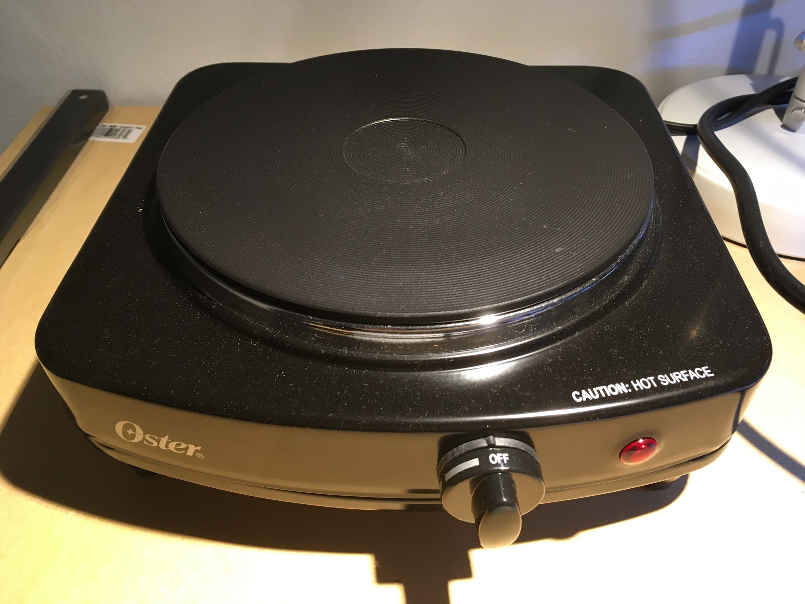
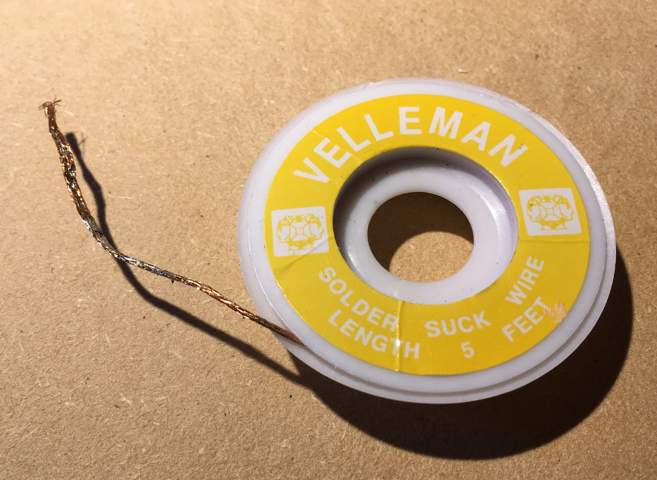
There are a few pieces of equipment that are necessary for the method presented here:
The technique varies based on the size of the pads being tinned. For small, isolated pads, place the tip of the soldering iron flat on the pad to heat it to soldering temperature. Feed solder into the pad until a droplet forms and covers it entirely. Remove the iron and solder simultaneously. The pad should be covered with a small, round bubble of solder as in figure 12. If the solder bubble has a point or if there is a large amount of solder on the pad, brush the tip of the iron quickly across the solder bubble to remove the excess solder.
 |
| Figure 12. Properly tinned PCB pads |
For lines of small pads, such as those found on many IC footprints, it can be faster to build a ball of solder on the iron tip, then drag the ball across the pads. Solder bridges may form between pads as in figure 13. To clear these solder bridges, brush the tip of the iron perpendicular to the line of pads.
 |
| Figure 13. A solder blob bridges several contacts. It can be cleared by brushing the iron across the solder bridge. |
For very large pads, such as grounding pads on IC footprints, place the iron tip on the pad and feed in a small amount of solder. Spread this solder around the pad uniformly with the tip of the iron as in figure 14. It is important to control the amount of solder added to large ground pads because if there is too much solder, it can lift up the part and cause it to slide or tilt during rework.
 |
| Figure 14. Lightly tinned center ground pad to avoid displacing the component |
Placement
After all of the pads on the board have been tinned, place a small drop of solder flux onto each one.
This serves two purposes:
- Clean contacts - Flux removes oxides, allowing the joint to reflow properly.
- Temporarily adhere parts - Flux is slightly tacky, which means that it can be used to hold parts in place.
Use tweezers to place all components onto their corresponding pads as in figure 15.
 |
| Figure 15. Components placed on a tinned PCB |
To make placement more efficient, it is often useful to find the required components and put them into an organizer. It is also helpful to print out a drawing of the PCB and label it with part values to reference quickly as in figure 16.
 |
| Figure 16. PCB drawing labeled for reference during assembly |
Reflow
Industrial solder reflow uses a tightly controlled oven to follow an optimal temperature profile. These temperature profiles are designed to minimize thermal shock and to stay within the temperature limits of components.
[4] Profiles are specified as a series of ramps and holds, where the ramps follow set rates of temperature increase or decrease measured in ℃/s. There are four regions in a typical reflow profile:
- Preheat - The board is brought to a temperature that is well below soldering temperature but high enough that solvents in the flux evaporate. This stage prevents the violent evaporation of solvents at higher temperatures. The temperature ramp rate during this phase is typically limited to 3 ℃/s
- Soak - The board is held at a temperature somewhat lower than the melting point of the solder. This allows temperature to equalize between the board and different components.
- Reflow - The temperature is ramped to around 25 ℃ above the solder melting point and held there. A ramp of 2 ℃/s is typical of this phase and the board is usually held at the maximum temperature for around 20 seconds.
- Cool down - The board is cooled at a rate of around 4 ℃/s, allowing the solder to solidify.
 |
| Figure 17. Representative PCB reflow temperature profile |
In practice, a precise profile is difficult to follow with a manually controlled hot plate, but it is possible to approximate an appropriate profile.
The first step is to determine the appropriate reflow temperature setting for the hot plate. This is done by placing a tinned scrap PCB onto the hot plate and slowly ramping up the temperature until the solder liquifies and becomes shiny. Mark where this temperature setting is and turn the hot plate off.
Allow the hot plate to cool back to room temperature, then place the board onto the hot plate and turn it to a medium-low temperature. This simulates the preheat phase. Allow the board and hot plate to come up to temperature for several minutes to simulate the soak phase. Turn up the temperature to the previously determined reflow setting to simulate the reflow phase. After the solder liquifies, wait 20 seconds and then turn off the hot plate. Use a pair of pliers or tweezers to remove the board from the hot plate to cool. It may be necessary to leave the hot plate on longer after the solder liquifies depending on the solder used.
It is possible to refine the process by using an infrared thermometer to find appropriate temperature settings for the hot plate. To find the reflow set point, turn on the hot plate and adjust it so that its temperature is stable at 25 ℃ above the solder’s melting temperature. For leaded solder, an appropriate temperature might be 225 ℃. To find the set point for the simulated soak phase, repeat this procedure with a setpoint of 160 ℃. Test the upper setpoint using a scrap PCB to verify that the solder melts at the temperature it is expected to melt at and adjust the temperature setpoint as needed.
Inspection and Correction
After the board cools to room temperature, inspect it for parts that are not properly soldered. The most common problems are parts turning or sliding.
If any parts are incorrectly soldered, it is necessary to reflow either all or part of the board to correct them depending on the problem.
For small parts where only one joint has been formed, it is possible to use a fine tip soldering iron to manually re-solder.
 |
Figure 18. A SMD resistor that turned during rework
|
Hold the part lightly with tweezers and touch the tip of the soldering iron to the connected solder joint.
 |
| Figure 19. Desoldering an incorrectly reflowed resistor |
The part will come free.
 |
| Figure 20. Removed SMD resistor |
Move it to the correct location and hold it with tweezers while melting the solder ball on one of the pads to form a joint.
 |
| Figure 21. Re-soldering a SMD resistor by hand |
Repeat this for the other joint.
 |
| Figure 22. Corrected SMD resistor |
If a component has multiple incorrectly formed joints, it is necessary to heat it and the surrounding area of the board to soldering temperature so that it can be moved. This can be achieved either by following the hot plate reflow process to bring the entire board up to temperature or by using a hot air reflow gun to heat only the desired area. Once the component reaches soldering temperature, use a pair of tweezers to push it into place. Allow the board to cool and re-inspect the joint. If the entire board was heated to soldering temperature, re-inspect the entire board. If the component is small, it may be easier to remove it, place it again under a microscope, and then reflow it again.
Once the board looks visually correct, run electrical tests to verify that it works and make any further corrections that might be necessary.
Designing for Assembly
When designing PCBs to be assembled with this method, there are a few concepts to keep in mind to ease assembly.
Avoid BGA and QFN packages. These packages have pads that are entirely covered. This makes assembly more difficult because differences in solder ball size can prevent connections to some pins. Additionally, it is more difficult to inspect solder joints on BGA and QFN components because all joints are covered.
If a BGA package must be used, make sure that there are no straight-line connections between the center pad and any of the outside pins. The large center pad will wick all of the solder to its center, which makes it almost impossible to solder any pins connected to it without solder mask to block the solder flow. As an alternative, connect the outside pin to a via, route a trace on the bottom of the board, and connect it to another via in the middle of the center pad.
When designing with small passive components, make an effort to keep package sizes at 0402 or larger. Smaller packages become increasingly difficult to work with, especially when placed without a microscope.
Place components far enough apart that they can be accessed with a soldering iron to simplify any corrections that might need to be made after reflow.
References
[1]
https://www.circuitspecialists.com/blog/choosing-soldering-flux/
[2]
https://www.kester.com/products/product/245-flux-cored-wire/
[3]
https://www.sparkfun.com/tutorials/category/2
[4]
https://www.compuphase.com/electronics/reflowsolderprofiles.htm